Share this course’s details with your family and friends.
Essentials of Professional VLSI Digital Design Training
Essentials of Professional VLSI Digital Design Training in Bangalore Offered by myTectra is the most powerful Essentials of Professional VLSI Digital Design Training ever offered with Top Quality Trainers, Best Price, Certification, and 24/7 Customer Care.
Learn Virtually Anywhere. Get Started Essentials of Professional VLSI Digital Design Online Training Now!

20% Limited Time Offer
Learn Virtually Anywhere. Award-Winning Training Company.
High-Quality Training Awaits You
Join over 100000+ learners who have taken up training with myTectra. Get High-Quality Training, Certification, Best Price and 24/7 Customer Care.
Key Program Highlights:
- Delivering top-notch education to equip you with essential skills.
- Learn from industry experts with real-world experience.
- A thorough curriculum covering all necessary topics.
- Dedicated support to help you secure job placements.
- High ratings reflecting our commitment to quality.
- Hands-on experience through real-world projects.
- Personalized, engaging learning for better outcomes.




About Program
Thorough understanding of all commonly used Essentials of Professional VLSI Digital Design Training constructs, fortified through detailed analysis of simulations using specially designed reference code. Robust design techniques towards enhancing the reliability, performance, power, area and configurability that are key towards building a successful career in the Essentials of Professional VLSI Digital Design Training design field.
Labs/mini-projects tailored towards developing a systematic design approach, guided by clear instructions combining screen-shots and expert tips. At the End of the training, you will also receive Certification and official course material issued by myTectra. Let's start your career in RPA.
Curriculum:
Introduction, Key RTL Coding Considerations and Environment/Tool Familiarization:
Learning Objectives:
- Set expectations on the course objectives and the completion criteria.
- Lay a solid foundation for getting into detailed RTL learning exercises and related lab work.
- Develop familiarity with the lab/project execution environment based on LINUX OS.
Topics:
- Overview of course objectives and the lecture Topics planned to be covered in the course.
- Overview of labs and projects that the students will conduct hands-on in the LINUX environment.
- Overview of Verilog Primer Labs.
- Main RTL quality considerations that a professional RTL designer must keep in mind while coding.
Hands-on LABs:
- LAB1 : LINUX environment: Directory structure, basic commands, VI editor.
- LAB1 : Quick-and-dirty compile and simulation of RTL using open-source Icarus Verilog and Gtkwave.
- LAB1 : Compile RTL and bring-up simulations using ModelSim.
- LAB2.1 : Example Code overview of File/IO/VCD example
- Assignment: Execute LAB2.1
Essentials of Clocking, SystemVerilog Labs:
Learning Objectives
- Understand all fundamental aspects about clocking that a VLSI engineer must be aware of.
- Understand the concepts of File/IO/VCD operations in SystemVerilog and related syntax.
Topics Essentials of Clocking:
- Overview
- Duty-cycle
- Synchronous and asynchronous clocks
- Setup and Hold time, timing requirements
- Clock-tree, clock-tree cells
- Phase and path reconvergence.
Hands-on LABs:
- LAB2.1 : Bring up the lab exercises and complete the analysis of File/IO/VCD SystemVerilog example.
- LAB2.2 : Example code overview of behavioral Vs structural RTL and Blocking Vs Non-Blocking assignments, understand the expected code behavior.
- Assignment: Execute LAB2.2
Clock-gating and Synchronization, SystemVerilog Labs:
Learning Objectives:
- Understand the most commonly used clock-gating techniques in depth.
- Internalize the concept of synchronization, its background, techniques and related timings.
- Understand the difference between behavioral and structural coding styles.
- Internalize the concepts of blocking and non-blocking assignments, and their usage.
Topics:
- Clock-gating:
- Need for clock-gating.
- Simple AND based clock-gating and related timing diagrams.
- Latch + AND based clock-gating circuit, related timing diagrams and DFTM consideration.
Synchronization:
- Sources of timing failures across asynchronous clock boundaries and the need for synchronization.
- Typical 2-stage synchronizer circuit and related timing diagrams.
- An example of how selective synchronization can be deployed across asynchronous boundaries, explained using timing diagrams.
- The concept of MTBF and how MTBF can be improved using a 3-stage synchronizer, explained using timing diagrams.
Hands-on LABs:
- LAB2.2 : Bring up the lab exercises and complete the analysis of the SystemVerilog examples for behavioral Vs Structural coding and blocking Vs non-blocking assignments
- LAB2.3 : Example code overview of signal drive strengths, functions, 'case', 'if' and conditional assignments, understand the expected code behavior.
- Assignment: Execute LAB2.3
Resets, Bus Interfaces and Side-band Signals, SystemVerilog Labs:
Learning Objectives:
- Understand the behavior and usage of synchronous and asynchronous Resets in detail.
- Familiarize the concept of Bus Interfaces and most popular examples.
- Familiarize the most commonly used side-band signals in an IP/SOC design that all VLSI designers must be aware of.
- Thorough review of the concept of Signal Drive Strengths and supported signal drive levels in SystemVerilog.
- Learn the syntax and usage of the three main behavioral constructs in SystemVerilog viz. 'case, 'if' and conditional-assignments.
- Understand the usage of functions in SystemVerilog.
Topics Resets:
- Overview of resets and various uses of resets.
- The key attributes of asynchronous reset.
- The key attributes of synchronous reset.
- The circuit, timing diagrams & code-snippets for asynchronous & synchronous resets.
Bus Interfaces:
- Overview of bus interfaces
- Common bus protocols
- Bus masters and slaves
Typical Side-band signals:
- Interrupts and events
- Clock and power management signals
- IO control signals
- Emulation and DFTM control signals
Hands-on LABs:
- LAB2.3 : Bring up the lab exercises and complete the analysis of the Verilog examples for signal drive strengths, functions, case, if and conditional assignments
- LAB2.4 : Example code overview of Verilog operators and forever/repeat/while loops, understand the expected code behavior.
- Assignment: Execute LAB2.4
Finite State Machines and Power Management Techniques, SystemVerilog Labs:
Learning Objectives:
- Study the difference between Moore and Mealy styles of FSM implementation.
- Familiarize with the objectives, the techniques used and most commonly used components of Power Management in IPs and SOCs.
- Get in touch with a complete list of all SystemVerilog operators.
- Understand in depth how 'foreach', 'repeat' and 'while' loops are used and how the simulator schedules the iterations.
Topics Finite State Machine (FSM):
- Overview and different representations.
- Two types of Finite State Machine implementations: Moore and Mealy.
- Power Management Techniques:
- Main objectives of implementing power management in SOCs
- Commonly used Power management techniques
Key components used for implementation of Power management:
- Voltage Level shifters
- Retention flip-flops
- Power switches
- Isolation cells
Hands-on LABs:
- LAB2.4 : Bring up the lab exercises and complete the analysis of the examples for all SystemVerlog operators and 'forever'/'repeat'/'while' loops.
- LAB2.5 : Example code overview of User Defined Primitives, tasks and SystemVerilog parameters, understand the expected code behavior.
Assignment: Execute LAB2.5
Power-Performance-Area (PPA) Trade-Offs, SystemVerilog Labs and Perl quick-start:
Learning Objectives:
- Familiarize with the concept of Power-Performance-Area (PPA) trade-offs and most commonly used knobs for achieving the PPA balance.
- Learn the syntax and usage of User Defined Primitives (UDP)
- Get introduced the Perl coding fundamentals and typical use-case scenarios
Topics Power-Performance-Area (PPA) trade-offs:
- Various knobs that VLSI designers use to balance the Power, Performance and Silicon Area of a device to achieve the optimal requirements. These include:
- Cell sizing
- Voltage domains
- Power domains
- Logic cloningUnderstand the impact of changing each knob on the PPA aspects of the device.
Hands-on LABs:
- LAB2.5 : Bring up the lab exercises and complete the analysis of the Verilog examples for User Defined Primitives, tasks and Verilog parameters.
- LAB2.6 : Example code overview of usage of compiler directives in Verilog, understand the expected code behavior.
- LAB3 : Review the Perl example that generates Shift Register SystemVerilog code in order to understand the basic usage of Perl and discuss the Perl exercises.
- Assignments: Execute LAB2.6 and LAB3
Design For Test and Manufacturability, SystemVerilog Labs and Perl quick-start:
Learning Objectives:
- Familiarize with the background and techniques related to Design For Test and Manufacturing (DFTM).
- Understand scan-chain operation in detail.
- Understand the purpose of ATPG Stuck-At, At-Speed, Boundary-Scan and IDDQ tests which are must-support basic DFTM tests for all devices.
- Familiarize with the usage of compiler directives in SystemVerilog.
- Fully analyse the Perl quick start exercises to lay a solid foundation for deeper learning and future application of Perl programming.
Topics Design For Test and Manufacturability (DFTM):
- The background of deploying extensive DFTM techniques in modern day designs.
- Most commonly used DFTM techniques and the major steps involved in accomplishing the DFTM implementation
- A detailed analysis of the scan-chain operation that forms the basis of most DFTM tests.
- ATPG Stuck-At, At-Speed, Boundary-Scan and IQQQ tests, related test coverage requirements and DPPM impact.
Hands-on LABs:
- LAB 2.6 : Bring up the lab exercises and complete the analysis of the Verilog example of compiler directives in SystemVerilog.
- LAB3 : Analyse the simulation results of the Perl generated SystemVerilog code. Review the reference Perl code that meets the requirements of the shift register code-generator exercise.
- LAB4 : Review the pattern detect example implementations of Moore and Mealy FSMs. Discuss the requirements of the FSM implementation expected to be done as part of the exercise.
- Assignments: Execute LAB4 exercise
IP/SOC Design Flows and Gate-Netlist generation Flows - Overview, Synthesis Labs:
- Familiarize with various stages and interdependencies of Industry standard IP and SOC development flows at a high-level.
- Understand the major steps involved in the generation of gate-netlist from RTL.
- Thorough understanding of FSM coding styles through execution and analysis of hands-on exercises.
- Get introduced to logic synthesis and leaf-cell libraries.
- Understand how RTL gets mapped to gate-level implementation by means of schematic analysis.
- Various stages of IP Development cycle from Specification to IP packaging.
- Various stages of SOC development cycle from Specification to Tape-out.
- A typical SOC block-diagram showing IP blocks and interface buses
- The three major steps in the gate-netlist generation:
- Logic synthesis process
- Scan insertion in the gate-netlist
- Formal Verification (Equivalence checks)
- LAB4 : Bring up the lab exercises and complete the analysis of the FSM design that is expected to be completed as part of the exercise.
- LAB5 : Review the RTL codes for the shift register and the Mealy FSM implementation that are planned to be taken through the synthesis experiments.
- LAB5 : Walk through the logic synthesis flows for the shift register code implementation and schematic review of the resultant gate-netlist.
- LAB5 : Understand the concept of leaf-cell library used during synthesis, using the TSMC018 .lib example.
- LAB5 : Discuss the synthesis experiment using the Mealy FSM Verilog code that is expected to be completed as part of LAB5 exercises.
- Assignment: Execute LAB5 exercises
Physical Design Flows and Semiconductor Manufacturing process - Overview, Synthesis Labs and Mini-Project1 start.:
Learning Objectives
- Familiarize with some of the must-know terminology and major stages of Physical Design implementation.
- Refresh the knowledge of silicon manufacturing cycle at a high-level. → Gain better understanding on how RTL gets mapped to gates through completing the synthesis exercises.
- Understand the requirements of the first mini-project in detail in order to prepare for implementation and touch-testing.
Topics Physical Design flows:
A quick snap-shot of various steps involved in converting a gate-netlist to the final tape-out database that goes to the manufacturing units. A typical SOC floorplan created during the physical design process.
Semiconductor device Manufacturing and Packaging:
A quick snap-shot of various stages of semiconductor manufacturing after the tape-out of the design, resulting in a packaged silicon device.
Hands-on LABs:
- LAB5 : Analyse the results of the synthesis experiment using the Mealy FSM Verilog code, which is expected to be completed as part of LAB5 exercises.
- LAB6 (Mini-Project) : Review the functionality requirements and reference templates required to implement the shift-pattern detect based counter design. Discuss the usage of a simple testbench in doing a sanity check of the design implementation.
- Assignment: Start execution of the LAB6 mini-project
AMBA APB and AXI4-Lite Bus Interfaces, Mini-Project1 follow-on and Mini-Project2 start:
Learning Objectives
- Understand in depth the two most commonly used bus interface for IP MMR programmation - The AMBA AXI4-Lite and APB.
- Build confidence through analysis of the reference design implementation for the first mini-project.
- Understand the requirements of the second mini-project in detail in order to prepare for implementation and touch-testing.
Topics
- AMBA APB and AXI4-Lite Interfaces:
- Introduction to AMBA APB and AXI4-Lite Bus interface signals
- Typical write and read transaction timing diagrams.
Hands-on LABs:
- LAB6 (Mini-Project1) : Analyse the reference implementation of the shift pattern detect based counter implementation and analyse the expected behavior of the design using simple testbench.
- LAB7 (Mini-Project2) : Review the implementation requirements of a PWM IP with APB MMR interface and programmable period, which is expected to be completed as part of the LAB7 mini-project .Walk through the reference templates and sample testbench that can be used for completion of the LAB7.
- Assignments: Take Mini-Project1 to completion, Execute LAB7 mini-project
Pointers for further learning and Online resources, Review of the Mini-Projects:
Learning Objectives → Share information on some useful WEB resources
Final review of the two Mini-Projects
Topics
- List of useful WEB resources for further learning and reference.
Hands-on LABs:
- LAB6/LAB7 Mini-Projects : Complete analysis of the final implementations of the designs and the simple testbenches that test the basic functionality of the two designs. Suggestions for further enhancements to the designs that can be executed off-line.
Join the Course Now!
Learning Path
Master new skills to achieve your career goals.
Demo Session
Participate in a demo session for an overview of the course content. You will meet instructors and fellow learners, ask questions, and understand the teaching approach, helping you gauge the course’s relevance to your goals.
Enrollment
Complete your registration to join the course. You will gain access to the Learning Management System (LMS), where all materials, schedules, and resources are available, ensuring you’re ready to embark on your learning journey smoothly.
Live Classes
Engage in live classes led by experienced instructors covering core topics in depth. Interactive discussions and Q&A sessions encourage active participation, enhancing your understanding and retention of the material taught.
Hands-On Project
Complete a hands-on project that applies your learned skills in practical scenarios. This project simulates real-world challenges, allowing you to build a portfolio piece that showcases your competencies to potential employers.
Certification
After completing the course and project, you will receive a recognized certification that validates your expertise and enhances your professional credentials in your chosen field.
Career Support
Access career support services after certification, including resume workshops, interview preparation, and job placement assistance. These resources equip you with the tools needed to transition successfully into the workforce.
Clients Testimonials
Hear what our students say about myTectra


Hear from Our Successful Learners!
Discover how myTectra transformed their careers—your success story could be next!
Course Features
Expert Trainers
Courses are delivered by experienced working professionals and subject matter experts with real-world experience.
Hands-On Training
We provide learners with practical experience through real-world scenarios, projects, and interactive exercises.
Customizable Corporate Training
Tailored training solutions designed to meet the specific needs of organizations and teams.
Certifications & Assistance
Certifications offered by myTectra align with international standards and we also help you to prepare for globally recognized certifications.
Global Recognition
Trusted by individuals and enterprises worldwide, with a track record of successful alumni and partnerships.
24 x 7 Expert Support
We have a 24x7 online support team to resolve all your technical queries, through a ticket-based tracking system, for a lifetime.
Gain prestigious credentials and recognition
Start Learning Today. Access Your Resources for a Lifetime!
Enjoy lifetime access to myTectra’s Learning Management System (LMS), including session recordings, study materials, and resources. This ensures continuous learning and easy reference to course content even after completion.
Resume Preparation Made Professional and Impactful
Get expert guidance in crafting a professional and impactful resume. myTectra’s resume-building support helps highlight your strengths, certifications, and skills effectively, increasing your chances of landing your dream job.
Prepare for Success with Expert Mock Interviews
Prepare for real-world interviews with personalized mock interview sessions conducted by industry experts. Receive feedback on your performance, learn key interview techniques, and gain the confidence to succeed in job interviews.
FAQs
Would you like to reach us for the training for your team? Please fill the below form. We will get back to as soon as possible.
myTectra is providing 100% placement assistance on our key courses. We help you with the career counselling, Exams on Key courses, Mock Interviews and Technical Interviews Tips.
Landing an interview proves that you have the job-specific skills for the position, but how do your interview skills stack up? Also, Soft skills are often the most important factor in showing you're the best candidate for the job.
Hence we are conducting FREE TRAINING on Soft-Skills worth Rs-25, 000 to all myTectra students which will help you to attend the interviews with more confidence.
You will never miss a lecture at myTectra. You can choose either of the two options:
Classroom Training:
- If you miss one or few classes we can give a backup class based on trainer and your convenient time.
- In case if you miss many classes, we can reschedule your class with upcoming batches or other running batches based on how many courses topics you have completed so far.
Live-Online Training:
- View the recorded session of the class available in your LMS.
- You can attend the missed session, in any other live batch.
Yes. We arrange a free demo for all the courses either in the Classroom or Live-Online demo. Please fill the demo request form below to schedule a free demo.
Just give us a CALL at +918047112411 OR email at support@mytectra.com
- Visa Debit/Credit Card
- American Express and Diners Club Card
- Master Card
- PayPal
- Net Banking/Wire Transfer
- UPI Payment such as Google Pay, PhonePe, Paytm
- Cash/Cheque/DD ( Not for Online Training )
For Individual:
Classroom Training - Bangalore
Live-Online Training - Globally
For Corporates:
Classroom Training - We deliver classroom training for corporate in more than 20 countries. Send us an Enquiry Now!
Online Training - Globally
* All of the classes are conducted live online. They are interactive sessions that enable you to ask questions and participate in discussions during class time. We do, however, provide recordings of each session you attend for your future reference.
Our Trainer’s are chosen not only for their knowledge and expertise but also for their real-time experience in the respective courses.
Build Real-World VLSI Design Skills with myTectra’s Hands-On Training Program
Related Programs
Career Services

Placement Assistance
Exclusive access to myTectra Job portal
Mock Interview Preparation
Resume & LinkedIn Profile Building

Access to Soft Skill Enhancement
One-on-one career guidance
Related Blogs
Explore Insights and Tips for Essentials of Professional VLSI Digital Design

Everything You Need To Know About ELK Stack Training

Revolutionizing Automation: How Vision Control Systems Are Shaping the Future of Manufacturing
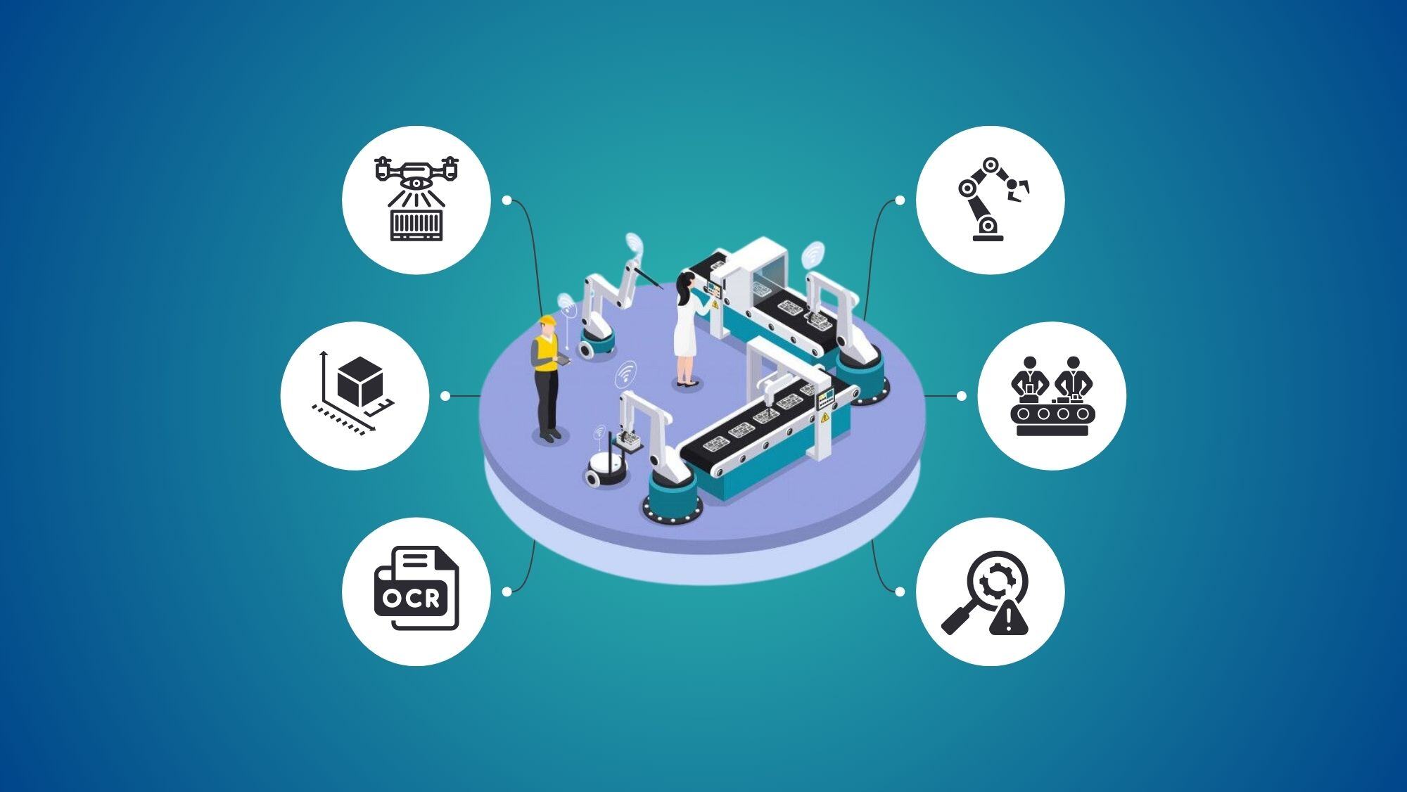
From Inspection to Automation: Top Applications of Vision Control Systems in Industry 4.0
Find Essentials of Professional VLSI Digital Design Course in Other Cities
Essentials of Professional VLSI Digital Design Training Online
myTectra offers top-quality Essentials of Professional VLSI Digital Design training with expert mentors and hands-on projects.
Essentials of Professional VLSI Digital Design Certification Course Online
Gain real-world skills in digital logic, HDL, and synthesis with this certification course designed for all experience levels.
Advanced Essentials of Professional VLSI Digital Design Training
Master advanced digital design concepts, RTL coding, verification, and synthesis with myTectra’s VLSI training curriculum.
Best Essentials of Professional VLSI Digital Design Online Course
Enroll in the best online course for VLSI Digital Design at myTectra, featuring flexible schedules and real-industry design labs.
Essentials of Professional VLSI Digital Design Training with Placement
Launch your VLSI career with myTectra’s placement-backed course featuring practical simulations and resume-ready projects.
Essentials of Professional VLSI Digital Design Training in Bangalore
Get trained in VLSI Digital Design by industry experts in Bangalore or online from anywhere, with career-focused learning paths.


