Altium PCB Design Training

Hands-On Altium PCB Design Training for High-Precision Circuit Development

Gain practical expertise in schematic creation, multilayer PCB layout, routing, and design validation using Altium Designer. Start building industry-ready PCB design skills today!

4000+ Learners
Expert Trainers
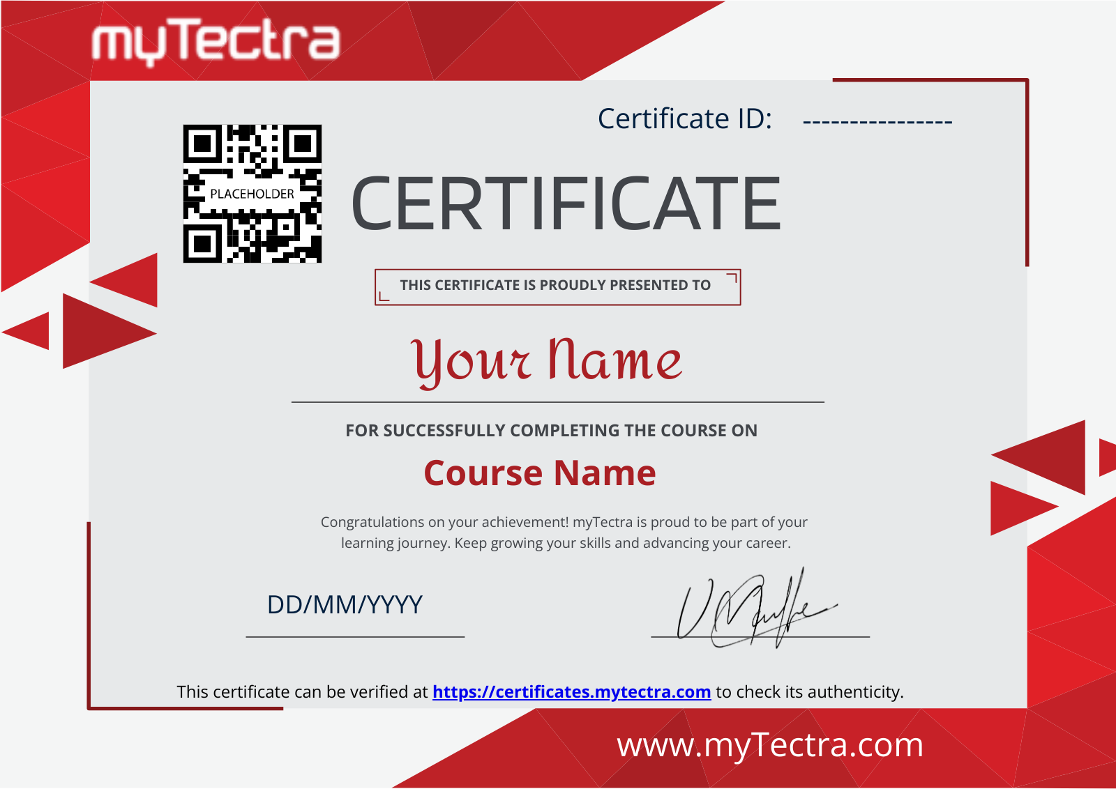
Verified Certificates
Realtime Projects
Individual Focus
Flexible Schedule
_altium-pcb-design-training-mytectra

20% Limited Time Offer

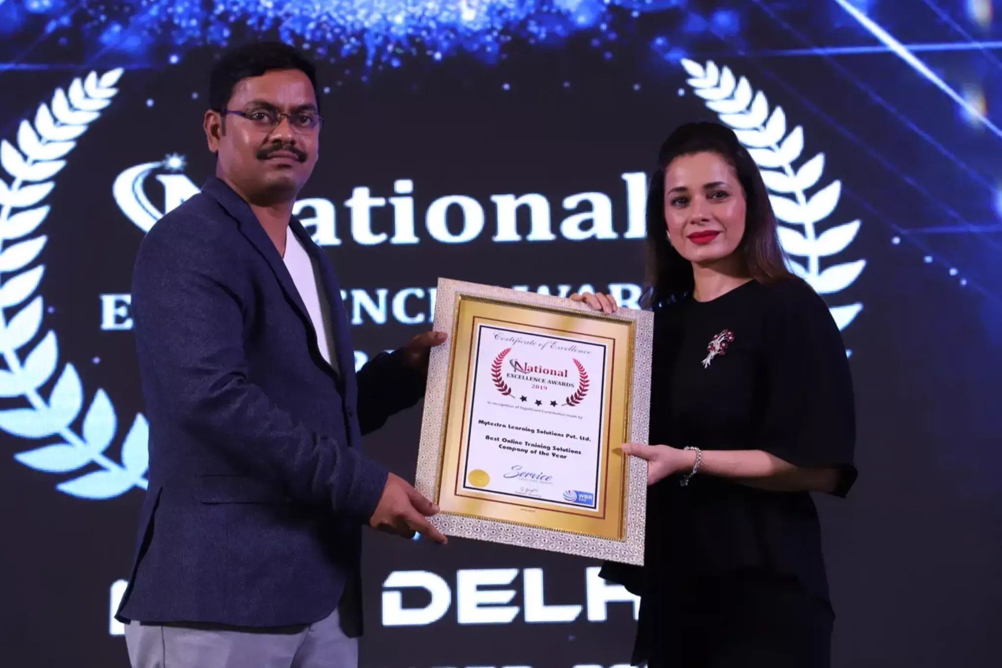
Learn Virtually Anywhere. Award-Winning Training Company.

High-Quality Training Awaits You

Join over 100000+ learners who have taken up training with myTectra. Get High-Quality Training, Certification, Best Price and 24/7 Customer Care.

Key Program Highlights:

  • Delivering top-notch education to equip you with essential skills.
  • Learn from industry experts with real-world experience.
  • A thorough curriculum covering all necessary topics.
  • Dedicated support to help you secure job placements.
  • High ratings reflecting our commitment to quality.
  • Hands-on experience through real-world projects.
  • Personalized, engaging learning for better outcomes.
awards-icon
Start Learning with the Best!
Join our award-winning courses today and take your skills to the next level.
Enroll Now!

About Program

The Altium PCB Design Training by myTectra is a comprehensive, hands-on training program designed to equip learners with the skills needed to design industrial-grade PCBs using Altium Designer, one of the most powerful and widely-used EDA tools in electronics product development.

This course takes participants through the complete PCB design cycle — from electronic fundamentals & schematic design to layout, routing, simulation, manufacturability, and fabrication outputs. The training includes real-time project development, design rule checks, best practices for EMI-EMC, and DFM (Design For Manufacturing) processes followed in industry.

By the end of the training, learners will be able to design production-ready PCB boards used in embedded systems, IoT devices, power electronics & consumer electronics.

Participants should have:

  • Basic understanding of Electronics (components, circuits)
  • Ability to read circuit diagrams

Preferred (Not Mandatory)

  • Knowledge of Ohm’s Law, power supply basics
  • Familiarity with microcontrollers & embedded systems

(No previous PCB / Altium experience required — training starts from basics.)

Technical Outcomes

  • Use Altium Designer for complete PCB workflow from schematic → layout → fabrication
  • Build and manage component libraries including footprints & 3D models
  • Apply PCB rules & constraints and perform DRC & LVS verification
  • Design multi-layer boards with high-speed routing awareness
  • Generate fabrication and assembly documentation for manufacturers

Professional Outcomes

  • Work confidently as PCB / Hardware Design Engineer
  • Create production ready PCB designs for industry
  • Review, optimize and debug existing PCB designs
  • Understand vendor communication for fabrication & assembly

Job Opportunities

  • PCB Design Engineer
  • Hardware Design / R&D Engineer
  • Embedded System Hardware Developer
  • Layout Design Engineer
  • Electronics Product Developer


  • Electronics / Electrical / Mechatronics Engineers & Students
  • Embedded / Hardware Engineers & Technicians
  • PCB Design Engineers and CAD layout engineers
  • R&D/Testing engineers needing PCB understanding
  • Makers & IoT product developers

Curriculum:

Module 1: Introduction

  • Introduction to Electronics and modern technologies
  • What is a Printed Circuit Board?
  • Types of PCB Designs (Single-layer, Double-layer, Multi-layer, Flex, Rigid-Flex, High-Speed)
  • Concept of EDA (Electronic Design Automation) Tools
  • PCB as part of product development lifecycle

Module 2: Design Specifications

  • Understanding PCB Design & Architecture
  • Floorplanning & project workflow
  • Logic Synthesis & partitions
  • EDA Databases, Simulation basics
  • Power analysis & optimization considerations
  • Place & Route methodology
  • Design for Manufacturability (DFM)
  • Design Closure
  • Design Rule Checking (DRC)
  • LVS (Layout vs Schematic)
  • Layout extraction and validation
  • Automatic Test Pattern Generation & testability guidelines

Module 3: Analog & Digital Electronics Fundamentals

  • Types of Power Supplies and selection criteria
  • Power supply component selection according to load
  • Analog circuits and applications
  • Practical interfacing of analog devices
    • BJT, FET, MOSFET, OP-AMP
  • Designing transistor-based circuits (BJT / FET / MOSFET)
  • OP-AMP introduction & practical applications
  • Components selection based on specifications and PCB location (thermal / safety / tolerance)

Module 4: Industrial Component Packages

  • Importance of component packaging in PCB design
  • Types of packages: THD, SMD, BGA, QFN, SOIC, DFN, SOT
  • Reading datasheets for mechanical dimensions & pad layouts
  • Designing footprints from datasheets
  • Tolerances, solder mask, paste mask

Module 5: Schematics in Altium

  • Introduction to Altium Design Environment
  • Basic schematic rules & best practices
  • Design flow & schematic connectivity management
  • Component Information Server
  • Managing parts & libraries (SCH + PCB + 3D packages)
  • Editing tools handling
  • Adding text and graphics
  • Creating new custom symbols
  • Print & plotting
  • Netlist creation & editing
  • DRC & processing of schematic design

Module 6: PCB Layout Design

  • Concept of ECO (Engineering Change Order)
  • Translating schematic to PCB layout
  • Managing footprints & libraries
  • Creating custom footprints
  • PCB dimensioning & stack-up creation
  • Routing:
    • Manual routing techniques
    • Multi-layer routing
    • High-speed routing basics
    • Differential pair & length tuning
  • Auto placement and auto routing
  • Copper pouring & thermal relief
  • Smart routing optimization
  • Drill management, via selection
  • DRC & back-annotation to schematic
  • PCB for manufacturing & assembly review

Module 7: Simulation in PCB Design

  • Concept and reliability of circuit simulation
  • Tools & design editing for simulation
  • Waveform analysis
  • Simulation models & signal integrity basics
  • Check-points & verification stages

Module 8: Fabrication Outputs & Documentation

  • Post-processing and generating production files
  • Gerber, NC Drill, Pick & Place, FAB notes
  • BOM generation and formatting
  • 3D PCB visualization & mechanical checks
  • Final project review

Final Capstone Project

A complete project including:

  • Schematic creation
  • Library development
  • PCB layout optimization
  • Routing with DRC
  • Gerber generation
  • Manufacturing package delivery
pdf-icon
Download the brochure
All details included
Download

Join the Course Now!

Path to Success

Learning Path

Master new skills to achieve your career goals.

Demo Session

Participate in a demo session for an overview of the course content. You will meet instructors and fellow learners, ask questions, and understand the teaching approach, helping you gauge the course’s relevance to your goals.

Enrollment

Complete your registration to join the course. You will gain access to the Learning Management System (LMS), where all materials, schedules, and resources are available, ensuring you’re ready to embark on your learning journey smoothly.

Live Classes

Engage in live classes led by experienced instructors covering core topics in depth. Interactive discussions and Q&A sessions encourage active participation, enhancing your understanding and retention of the material taught.

Hands-On Project

Complete a hands-on project that applies your learned skills in practical scenarios. This project simulates real-world challenges, allowing you to build a portfolio piece that showcases your competencies to potential employers.

Certification

After completing the course and project, you will receive a recognized certification that validates your expertise and enhances your professional credentials in your chosen field.

Career Support

Access career support services after certification, including resume workshops, interview preparation, and job placement assistance. These resources equip you with the tools needed to transition successfully into the workforce.

Clients Testimonials

Hear what our students say about myTectra

“I did the Python & Django course in myTectra. myTectra also gave me the opportunity to work on a real-time project which helped me a lot to get my concept throw. myTectra also provided me the placement in the company for the course I did in mytectra.”

prinjal
Prinjal
Python
“I am from Robert Bosch and have taken up Python Flask corporate training from myTectra. I am very much satisfied and happy with this customized training. The tutor was extremely helpful and flexible and provided the best insightful training.”

princy
Princy
Python Flask
“I have done Java Full Stack developer course in myTectra. myTectra has supported me in all possible ways. I have excellent knowledge of the course. mytectra has given all practical knowledge with real-time problems and examples”

sunita
Sunitha
Java Full Stack Developer

Hear from Our Successful Learners!

Discover how myTectra transformed their careers—your success story could be next!

Course Features

Expert Trainers

Courses are delivered by experienced working professionals and subject matter experts with real-world experience.

Hands-On Training

We provide learners with practical experience through real-world scenarios, projects, and interactive exercises.

Customizable Corporate Training

Tailored training solutions designed to meet the specific needs of organizations and teams.

Certifications & Assistance

Certifications offered by myTectra align with international standards and we also help you to prepare for globally recognized certifications.

Global Recognition

Trusted by individuals and enterprises worldwide, with a track record of successful alumni and partnerships.

24 x 7 Expert Support

We have a 24x7 online support team to resolve all your technical queries, through a ticket-based tracking system, for a lifetime.

Gain prestigious credentials and recognition

mytectra-certificate


Global Accreditation
Recognized Credentials

Start Learning Today. Access Your Resources for a Lifetime!

Enjoy lifetime access to myTectra’s Learning Management System (LMS), including session recordings, study materials, and resources. This ensures continuous learning and easy reference to course content even after completion.

Lifetime Access
24/7 Assistance

Resume Preparation Made Professional and Impactful

Get expert guidance in crafting a professional and impactful resume. myTectra’s resume-building support helps highlight your strengths, certifications, and skills effectively, increasing your chances of landing your dream job.

Job-Ready Resume
Resume That Stands

Prepare for Success with Expert Mock Interviews

Prepare for real-world interviews with personalized mock interview sessions conducted by industry experts. Receive feedback on your performance, learn key interview techniques, and gain the confidence to succeed in job interviews.

Simulate Real Interviews
Boost Your Confidence

FAQs

How do I contact myTectra for Corporate Training?

Would you like to reach us for the training for your team? Please fill the below form. We will get back to as soon as possible.

Will I get placement assistance?

myTectra is providing 100% placement assistance on our key courses. We help you with the career counselling, Exams on Key courses, Mock Interviews and Technical Interviews Tips.

Landing an interview proves that you have the job-specific skills for the position, but how do your interview skills stack up? Also, Soft skills are often the most important factor in showing you're the best candidate for the job.

Hence we are conducting FREE TRAINING on Soft-Skills worth Rs-25, 000 to all myTectra students which will help you to attend the interviews with more confidence. 

What if I miss a class?

You will never miss a lecture at myTectra. You can choose either of the two options:

Classroom Training:

  • If you miss one or few classes we can give a backup class based on trainer and your convenient time. 
  • In case if you miss many classes, we can reschedule your class with upcoming batches or other running batches based on how many courses topics you have completed so far.

Live-Online Training:

  • View the recorded session of the class available in your LMS.
  • You can attend the missed session, in any other live batch.
Can I attend a demo session before enrollment?

Yes. We arrange a free demo for all the courses either in the Classroom or Live-Online demo. Please fill the demo request form below to schedule a free demo.

What if I have more queries?

Just give us a CALL at +918047112411 OR email at support@mytectra.com

What are the payment options?
Payments can be made using any of the following options and a receipt of the same will be issued to you automatically via email for both classroom training and Online training.
 
  • Visa Debit/Credit Card
  • American Express and Diners Club Card
  • Master Card
  • PayPal
  • Net Banking/Wire Transfer
  • UPI Payment such as Google Pay, PhonePe, Paytm
  • Cash/Cheque/DD ( Not for Online Training )
Where do the classes take place?

For Individual: 

Classroom Training - Bangalore

Live-Online Training - Globally 

For Corporates: 

Classroom Training - We deliver classroom training for corporate in more than 20 countries. Send us an Enquiry Now!

Online Training - Globally

* All of the classes are conducted live online. They are interactive sessions that enable you to ask questions and participate in discussions during class time. We do, however, provide recordings of each session you attend for your future reference.

Who are the Trainers?

Our Trainer’s are chosen not only for their knowledge and expertise but also for their real-time experience in the respective courses.

Back to top
Ready to Start

Transform your hardware design expertise with Altium PCB Design Training from myTectra.

Related Programs

Adobe Customer Journey Analytics
4k+ LearnersLearn more →
Adobe Experience Platform
5k+ LearnersLearn more →
Adobe Experience Manager
10k+ LearnersLearn more →
Adobe Real-Time CDP
1k+ LearnersLearn more →
Adobe Analytics
7k+ LearnersLearn more →
Adobe Campaign Classic
8k+ LearnersLearn more →
Adobe Campaign
7k+ LearnersLearn more →
Adobe Target
2k+ LearnersLearn more →
Adobe Launch
2k+ LearnersLearn more →
Adobe Commerce (Magento)
2k+ LearnersLearn more →
Adobe Marketo Engage
2k+ LearnersLearn more →
Adobe Workfront Training
1k+ LearnersLearn more →
Adobe Audience Manager
1k+ LearnersLearn more →

Career Services

subscribe-mytectra
placement-icons
Placement Assistance
job-portal-icon
Exclusive access to myTectra Job portal
mock-interview-icon
Mock Interview Preparation
linkedin-icon
Resume & LinkedIn Profile Building
soft-skill
Access to Soft Skill Enhancement
career-guidance-icon
One-on-one career guidance

Land Your Dream Job Like Our Alumni

Related Blogs

Explore Insights and Tips for Altium PCB Design

Everything You Need to Know About PCB Design Training


Everything You Need to Know About PCB Design Training

Jul 29, 2023, 11:08:37 AM 4 min read
The Top 5 Common Mistakes to Avoid in PCB Design


The Top 5 Common Mistakes to Avoid in PCB Design

Jul 29, 2023, 11:07:18 AM 3 min read
Mastering PCB Design: Essential Tips and Tricks for Success
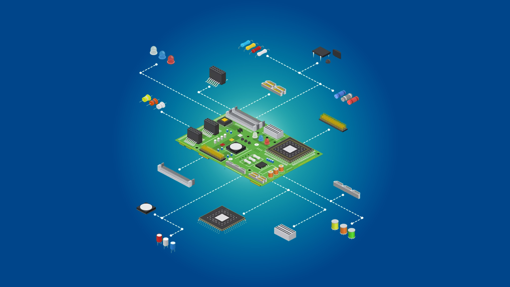

Mastering PCB Design: Essential Tips and Tricks for Success

Jul 29, 2023, 11:06:01 AM 2 min read

Find Altium PCB Design Course in Other Cities

Altium PCB Design Online Training

myTectra offers top-quality Altium PCB Design Online Training with expert instructors, real-world PCB projects, and industry-recognized certification.

Altium Designer Certification Course Online

Gain practical skills in schematic design, PCB layout, routing, and manufacturing workflows with myTectra’s Altium Designer Certification Course Online, suitable for all experience levels.

Advanced Altium PCB Design Training Online

Master high-speed design, multilayer PCB layout, impedance control, and DFM verification with myTectra’s Advanced Altium PCB Design Training Online.

Best Altium PCB Design Online Course

Join the best Altium PCB Design Online Course at myTectra, featuring flexible learning, expert mentorship, practical PCB assignments, and dedicated learner support.

Altium PCB Design Training Online with Placement

Kickstart your electronics design career with myTectra’s Altium PCB Design Training Online, offering placement assistance and hands-on circuit design projects.

Altium PCB Design Training in Bangalore

myTectra provides expert-led Altium PCB Design Training in Bangalore and globally online, helping you design professional, manufacturing-ready PCBs with confidence.