Introduction:
Printed Circuit Board (PCB) design is a complex and intricate process that requires careful planning, attention to detail, and a solid understanding of electronic principles. Even experienced designers can fall victim to common pitfalls that can lead to suboptimal performance, reliability issues, and costly delays. In this blog, we'll explore some of the most prevalent mistakes in PCB design and provide insights on how to avoid them, ensuring your PCB projects are smooth, efficient, and successful.
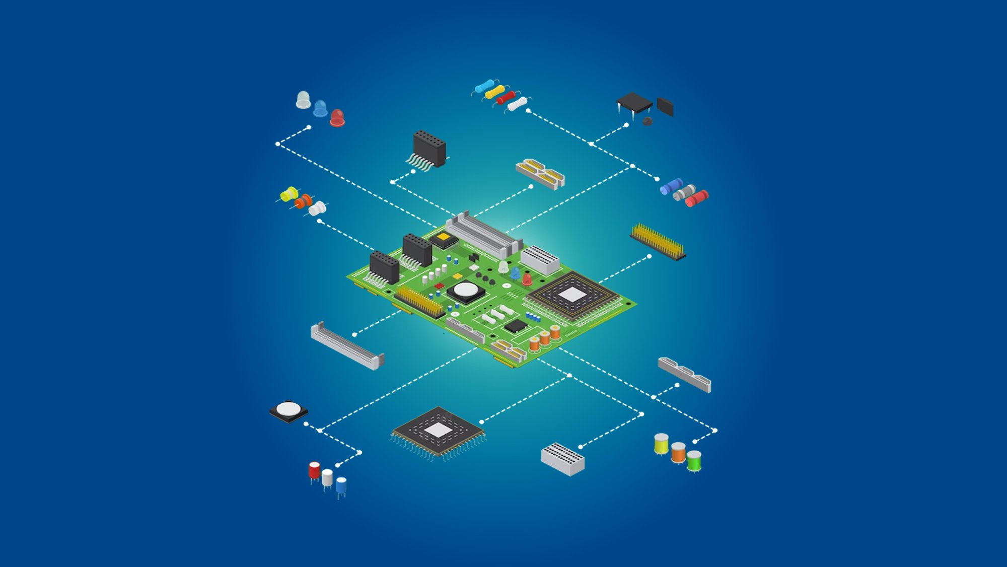
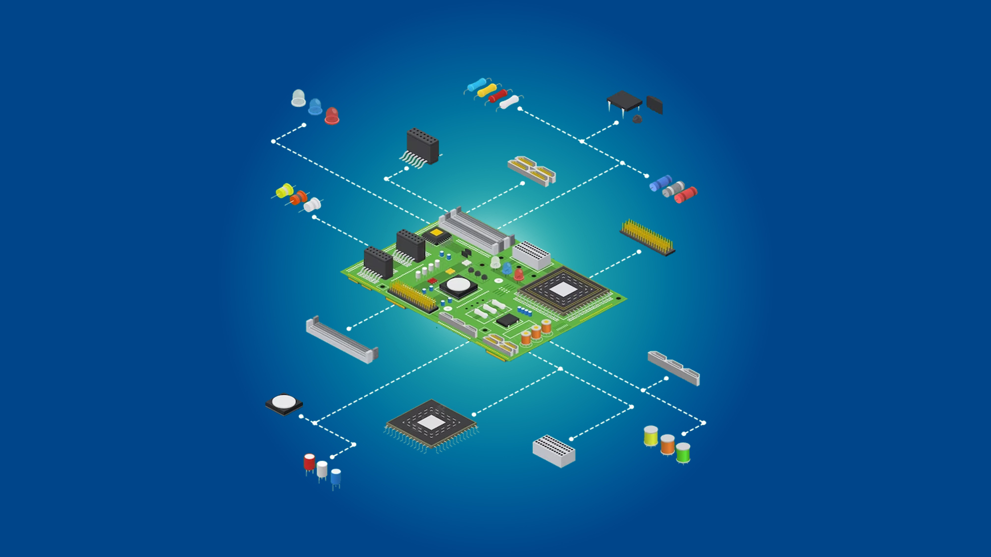
1. Neglecting Proper Component Placement:
One of the foundational aspects of PCB design is component placement. Poorly organized components can lead to signal integrity problems, increased electromagnetic interference, and difficulties in routing traces. To avoid this mistake, plan your component layout meticulously, grouping related components together and considering factors like signal flow, thermal management, and manufacturability.
2. Inadequate Trace Routing:
Routing traces on a PCB requires careful consideration to avoid signal degradation, crosstalk, and electromagnetic interference. Common routing mistakes include improper trace widths, insufficient clearance between traces, and improper ground plane design. Utilize design rule checks (DRC) and follow best practices to ensure proper trace routing for optimal signal integrity.

3. Overlooking Thermal Management:
Heat dissipation is a critical aspect of PCB design, especially for power-intensive components. Failing to address thermal management can lead to overheating, component failure, and reduced lifespan. Make use of thermal vias, heatsinks, and proper airflow to ensure efficient heat dissipation and maintain the reliability of your PCB.
4. Ignoring Design for Manufacturing (DFM) Guidelines:
Design for Manufacturing (DFM) considerations are essential to ensure that your PCB can be produced efficiently and cost-effectively. Neglecting DFM guidelines can lead to challenges during fabrication and assembly, resulting in delays and increased production costs. Familiarize yourself with your manufacturer's DFM guidelines and design your PCB with manufacturing in mind.
5. Disregarding Signal Integrity:
Signal integrity issues can lead to unpredictable behavior and poor performance of your PCB. Factors like trace length matching, impedance control, and proper grounding play a crucial role in maintaining signal integrity. Utilize high-speed design techniques and simulation tools to analyze and optimize signal paths, reducing the risk of signal integrity problems.
6. Underestimating EMI and EMC Concerns:
Electromagnetic Interference (EMI) and Electromagnetic Compatibility (EMC) issues can arise from improper PCB design practices, leading to problems like radio frequency interference and compliance failures. Pay close attention to grounding, shielding, and routing techniques to mitigate EMI and EMC challenges and ensure your PCB meets regulatory standards.
7. Skipping Prototyping and Testing:
Rushing into production without prototyping and testing is a recipe for disaster. Prototyping allows you to identify design flaws and performance issues before full-scale production. Use test equipment to verify signal quality, power distribution, and overall functionality. Iterating based on test results ensures that your final PCB design is robust and reliable.
8. Failing to Document Design Decisions:
Thorough documentation is often underestimated but is crucial for collaboration, troubleshooting, and future revisions. Keep detailed records of design decisions, component selections, and any modifications made during the design process. This documentation will be invaluable for yourself and others who work on the project in the future.
Conclusion:
Navigating the world of PCB design requires a combination of technical expertise, careful planning, and a vigilant eye for potential pitfalls. By being aware of these common mistakes and taking proactive steps to avoid them, you can significantly increase the likelihood of a successful and efficient PCB design process. Whether you're a novice or an experienced designer, embracing a methodical and detail-oriented approach will help you create PCBs that meet performance expectations, maintain reliability, and contribute to the success of your electronic projects.

Everything You Need To Know About Magento Training
Mastering PCB Design: Essential Tips and Tricks for Success

No Comments Yet
Let us know what you think